Feature #5071
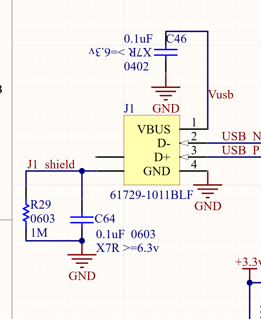
closeddifferent connection between USB shield and GND
100%
Description
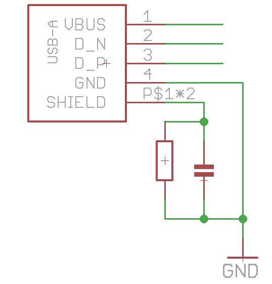
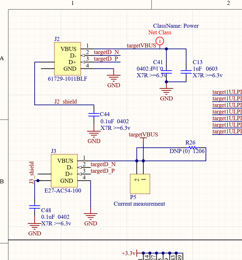
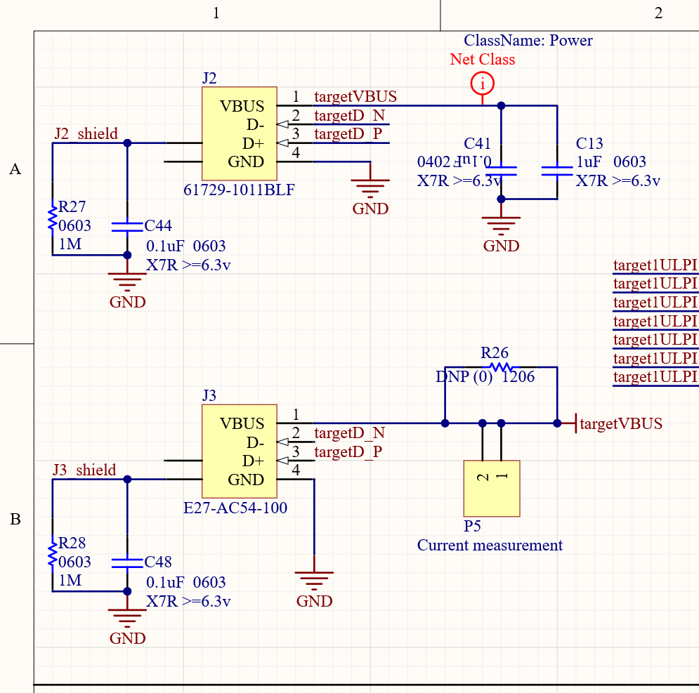
related to the way how GND is connected to the USB shields of J2 and J3:
Currently, there is only a capacitor (C44 and C48). We would like to- add a 1M resistor 0603 in parallel to the capacitor
- increase the footprint from 0402 to 0603 for C44 and C48
- currently there's a direct connection. let's use the same approach as for J2 and J3, i.e.
- capacitor and resistor in parallel between shield and GND
Files
Updated by laforge about 3 years ago
- Assignee changed from mschramm to cibomahto
Updated by cibomahto about 3 years ago
- File previous.png previous.png added
- File corrected.png corrected.png added
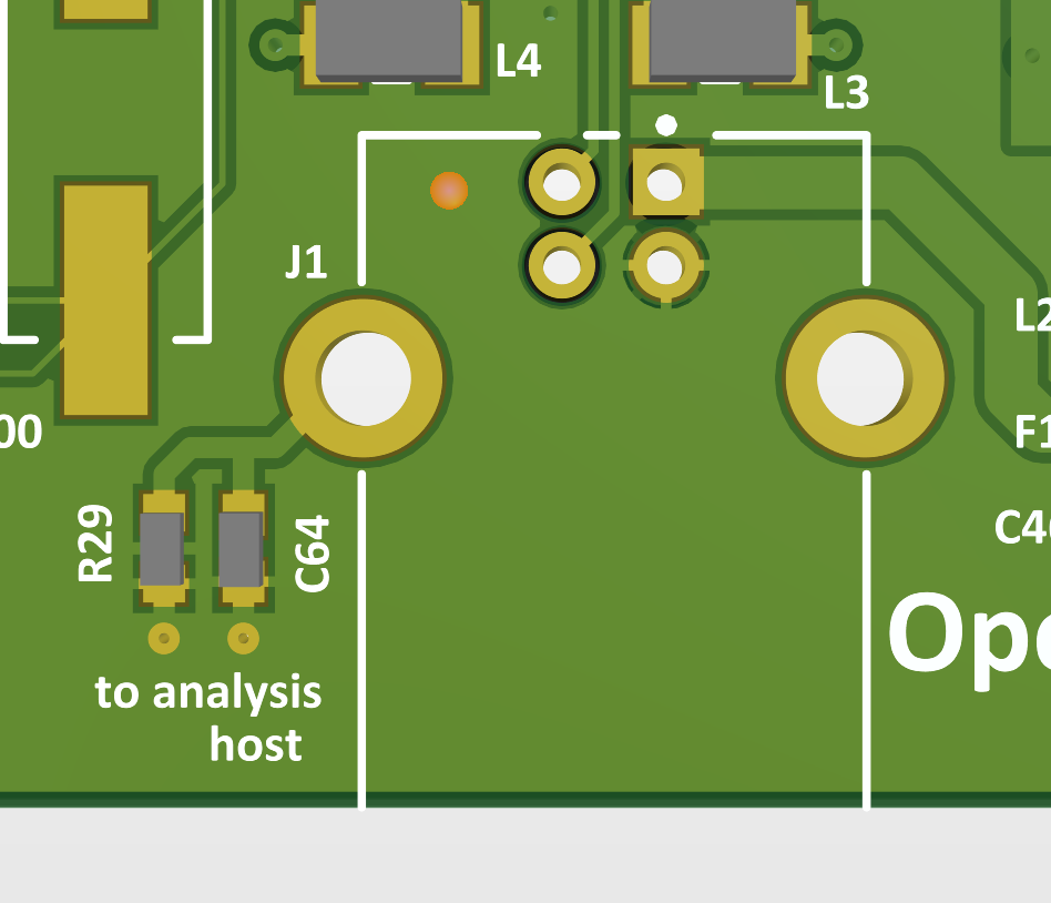
- File component placement.png component placement.png added
Implemented for J2 and J3
Updated by cibomahto about 3 years ago
- File J1 corrected.png J1 corrected.png added
- File component placement J1.png component placement J1.png added
Also for J1. Note that the shield filter components were only connected to one of the shield connector pins in the original design, so I did not modify this. If you'd prefer there to be a trace linking them on the board, please let me know.
Updated by cibomahto about 3 years ago
Updated by mschramm about 3 years ago
- Status changed from New to In Progress
cibomahto wrote:
Note that the shield filter components were only connected to one of the shield connector pins in the original design, so I did not modify this. If you'd prefer there to be a trace linking them on the board, please let me know.
No, I'm fine with this, as the USB receptacle's shield shall connect both THT solder pads anyways. As long as 'the other' pad is isolated from GND, it's ok.
Updated by mschramm about 3 years ago
- Status changed from In Progress to Resolved
- % Done changed from 0 to 100
solved, thanks

