Bug #5073
closedrepair single via restring rule violation
100%
Description
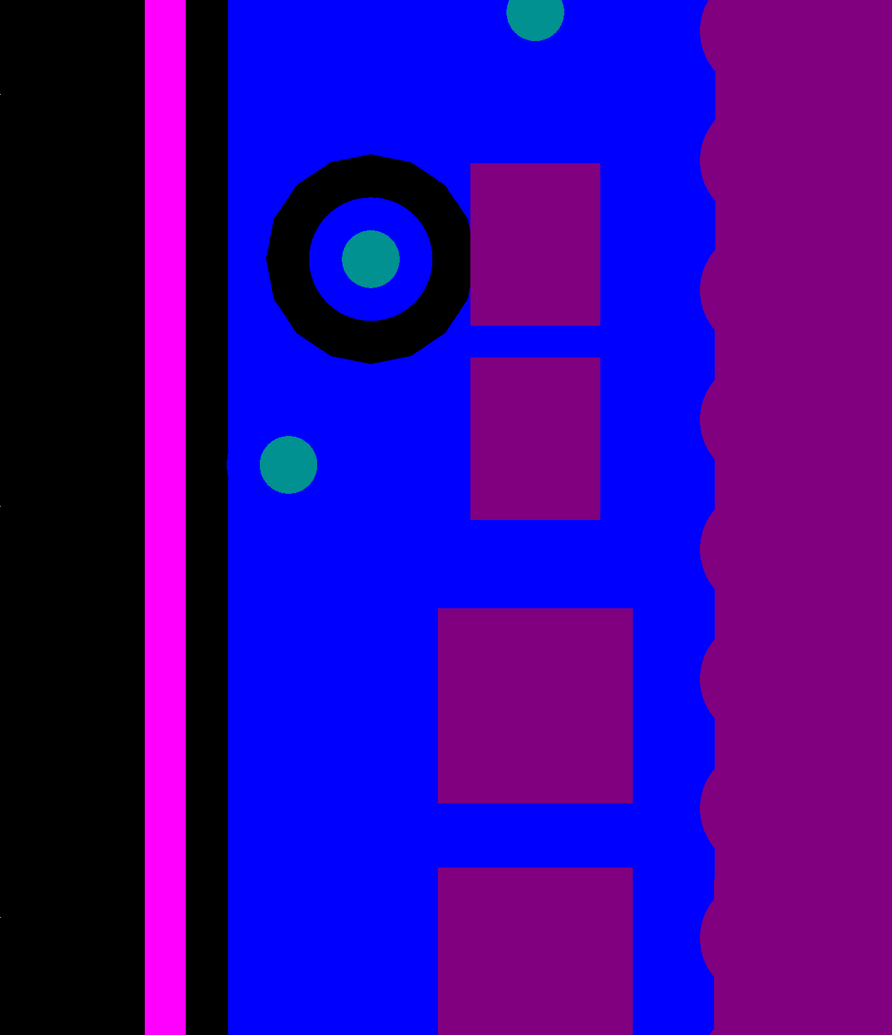
For the technology class we want to use for the upcoming production run, an inner and outer restring (annular ring) of at least 0,125mm is needed for the defined finished hole size for vias of 0,25mm. This is maintained all over the PCB - except in one spot (see image (animated gif)), on that spot the restring would only be 0,079 mm, and hence the pre-flight shows an error.
This could have been caused by different settings for e.g. min. distance of copper layers to PCB outline in your defaults over the ones in project. Likely the easiest way to repair this is to move that single via slightly more inwards - better than touching the design rules, but you decide.
(I'm going to report this in github too, it's just to keep track this issue also here.)

Files
| restring-violation.gif | View restring-violation.gif | 16.1 KB | |||
| Screenshot 2021-03-12 165534.png | View Screenshot 2021-03-12 165534.png | 14.7 KB | copper | ||
| Screenshot 2021-03-12 165906.png | View Screenshot 2021-03-12 165906.png | 36.7 KB | mininal outset | ||
| Screenshot 2021-03-12 170812.png | View Screenshot 2021-03-12 170812.png | 157 KB |


Updated by cibomahto about 3 years ago
No problem. I am using the project rules (they're mostly stored in the project files in Altium), however I'm using a significantly newer version of Altium than the project, so it's not surprising that there has been some drift. In particular the way that the board shape is defined has changed.
Is there a copy of the original production gerbers, for reference? I didn't see them in the project repo or associated sites.
Updated by cibomahto about 3 years ago
I'm a little confused now- that via looks like it has an annular ring of 0,2045, so even clipping off a significant portion of it shouldn't bring it under 0,079. I agree it's bad form to leave it hanging out past the plane fill, so I'll move it in. Please let me know if I'm missing something here.
Updated by cibomahto about 3 years ago
Updated by cibomahto about 3 years ago
Updated by mschramm about 3 years ago
cibomahto wrote:
I'm a little confused now- that via looks like it has an annular ring of 0,2045, so even clipping off a significant portion of it shouldn't bring it under 0,079.
This is because the inner layer demand more isolation clearance from the PCB outline (0,40mm (16mil)) than top and bottom copper (0,25mm (10mil)). So as the former have an outline closer to that via's center, they intersect the restring's area and hence their diameter.
Updated by cibomahto about 3 years ago
Ah, I see. Are the (0,40mm (16mil)) / (0,25mm (10mil)) the rules from your board house? I see that the project had a pullback distance of .508mm for the inner plane layers. The pullback on the top and bottom layers is defined in an obsolete way for Altium, but is effectively ~.4mm from the edge of the board, so both have some margin.
Updated by cibomahto about 3 years ago
- Status changed from New to In Progress
Updated by mschramm about 3 years ago
cibomahto wrote:
Are the (0,40mm (16mil)) / (0,25mm (10mil)) the rules from your board house?
yes, they are.
I see that the project had a pullback distance of .508mm for the inner plane layers. The pullback on the top and bottom layers is defined in an obsolete way for Altium, but is effectively ~.4mm from the edge of the board, so both have some margin.
OK, thanks, - I wasn't aware of this.
Updated by mschramm about 3 years ago
cibomahto wrote:
Is there a copy of the original production gerbers, for reference? I didn't see them in the project repo or associated sites.
No, there unfortunately is not - the Gerbers we got prior to your work were already generated subsequently.
Updated by mschramm about 3 years ago
- Status changed from In Progress to Resolved
- % Done changed from 0 to 100
has been solved, thanks

