Calypso Digital Baseband
- Table of contents
- Calypso Digital Baseband
- Variants
- DSP
- CPU
- MODEM UART
- IRDA UART
- RIF (Radio Interface)
- DPLL + clock block
- GEA (GPRS Encryption Algorithm)
- Watchdog timer === Interrupt Controller ===
- SIM card controller
- TSP controller (Time Serial Port)
- RTC clock
- ULPD (Ultra Low Power Device)
- I2C Master controller
- SPI Master controller
- TIMER1 / TIMER2 general purpose timers
- PWL (PWM for Light)
- PWT (PWM for Tones)
- JTAG Interface
- Debug traces
The Calypso Digital Base Band chip is a popular DBB implementation for inexpensive feature phones.
The register-level manuals seem to have leaked at some point and are available from cryptome.org
at http://cryptome.org/ti-calypso2.pdf and http://cryptome.org/ti-calypso1.pdf
As cryptome.org is currently suffering legal battles due to Microsoft stupidity,
you can use http://cryptome.quintessenz.org/mirror/ti-calypso1.pdf / http://cryptome.quintessenz.org/mirror/ti-calypso2.pdf
Variants
- Calypso G2 C035
- Calypso G2 C035 Lite (D751749GHH)
- Like C035, only 256kBytes of internal memory
DSP
More information on the DSP used in the Calypso DBB is available on HardwareCalypsoDSP.
CPU
The CPU embedded in the calypso chipset is a ARM7TDMI. Details documents about this CPU is available from the ARM infocenter at "h2. Memory Map
- nCS0 0x0000'0000 ... 0x007f'ffff (C123: external NOR flash)
- nCS6 0x0080'0000 ... 0x00bf'ffff (internal SRAM, in case of calypso lite only 256kBytes)
- nCS1 0x0100'0000 ... 0x017f'ffff (C123: external SRAM)
Integrated Peripherals
TPU (Time Processing Unit) =
- A programmable micro-engine clocked at GSM quarter-bit clock
MODEM UART
- The UART that is typically connected to a PC or the application processor in a smartphone
IRDA UART
- The UART that is either connected to IRDA or for diagnostics/programming
RIF (Radio Interface)
- Connects to the synchronous bi-directional BSP (Baseband Serial Port)
DPLL + clock block
- Generate clocks for DSP, ARM and all peripherals
GEA (GPRS Encryption Algorithm)
- Encrypts/Decrypts data according to the proprietary GEA algorithm
Watchdog timer ===
Interrupt Controller ===
Memory interface (SRAM/ROM) ===
DMA controller ===
- Only usable for UART and RIF, can only DMA to small API RAM memory region
SIM card controller
- Connects to the SIM card socket in the phone
TSP controller (Time Serial Port)
- Controls the TSP, which controls the sequencing of all external peripherals like ABB, RF chip, RF PA, Antenna Switch
RTC clock
- A pretty standard realtime clock
ULPD (Ultra Low Power Device)
- Responsible for enabling the phone to go to lowest-possible power mode while IDLE, but still waking up at the right point to receive important data (like paging channel) from the BTS
I2C Master controller
- Typically connects to external peripherals like LCD (if any)
- It assumes that the peripheral has an address byte. If your peripheral doesn't, you have to
write the first byte into the address register and not the FIFO - You cannot under-fill the FIFO, i.e. if you write 8 bytes into the 16byte deep fifo, the controller
will transmit 16 bytes rather than 8. Therefore, always limit the FIFO depth to your write size!
More details about this can be seen at HardwareCalypsoI2CFIFO"httpinfocenterarmcomhelpindexjsp.
SPI Master controller
- Connects to USP of ABB and possibly other external peripherals
TIMER1 / TIMER2 general purpose timers
The timer input clock is not mentioned in the data sheet. It seems to be 13MHz / 32, i.e. 406.25kHz
PWL (PWM for Light)
- connected to the screen/keypad backlight
PWT (PWM for Tones)
- connected to a buzzer for ringtone generation
JTAG Interface
The Calypso has an ARM7TDMI JTAG interface, which is exposed on phones like the Motorola C115] [wikiMotorolaC155 C155] [wikiSonyEricssonJ100i Sony Ericsson J100i] and the [wikiPirelliDPL10 Pirelli DP-L10.
With standard ARM JTAG debuggers like OpenOCD, halting the core does not work out-of-the-box, because ARM instruction 0xb needs to be executed first (which is an proprietary extension to the ARM7TDMI TAP-Controller). It is unclear what this instruction does exactly.
The OpenOCD configuration file along with the corresponding svf-file is attached to this page.
Debug traces
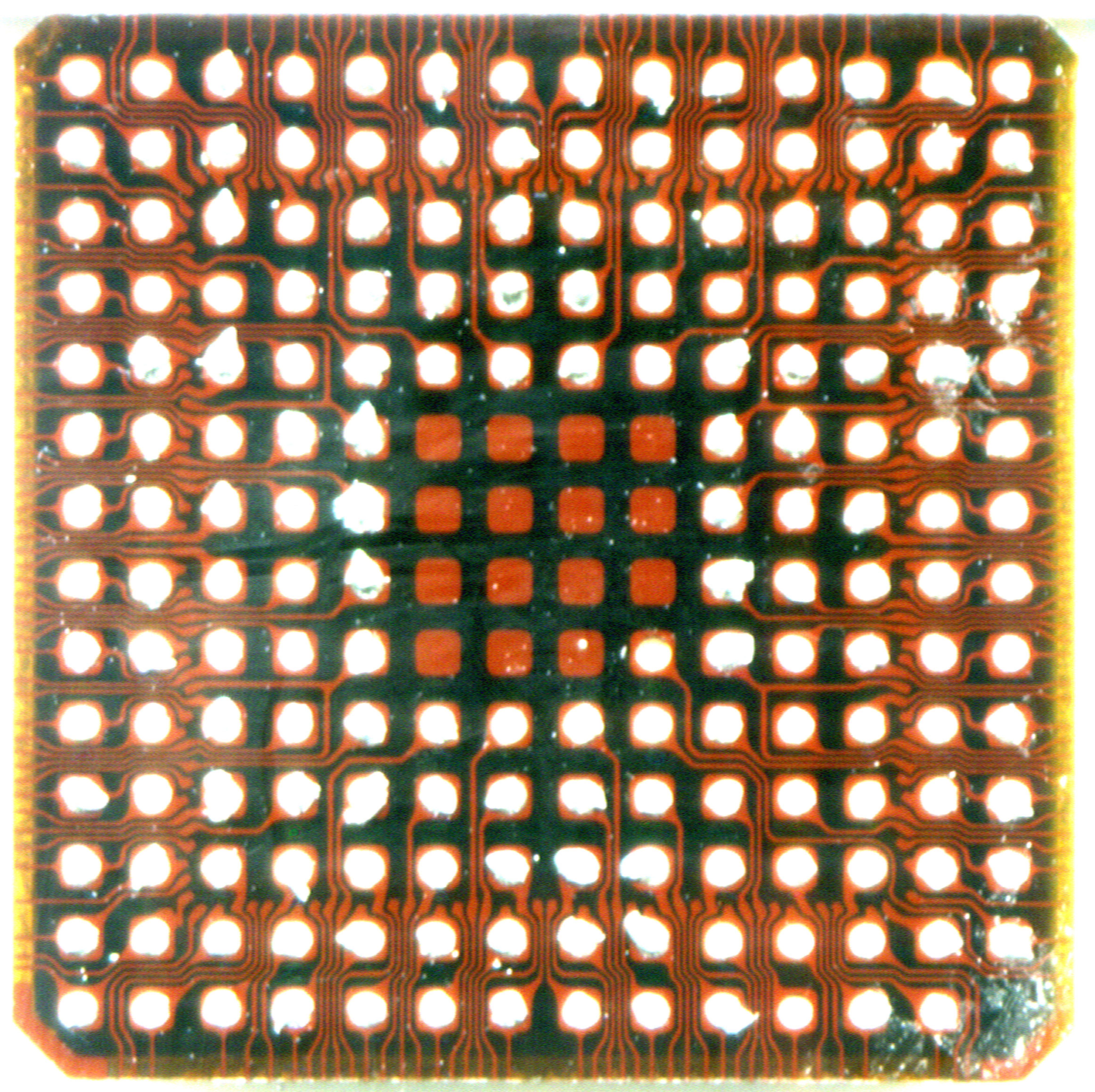
The chip has very tiny debug traces on a small flex-pcb around the 4 sides of the chip.
Which trace goes to which ball can be seen on this scan: http://www.steve-m.de/pictures/calypso_bottom.jpg
Updated by fixeria about 6 years ago · 16 revisions

